Info Draw The Circuit Diagram Of Ttl Nand Right Of Entry Now
39+ Easy Tutorial draw the circuit diagram of ttl nand right of entry Online
Activity: TTL inverter and NAND admittance - Analog Devices Wiki
25 Jun 2020 The schematic of a Transistor Transistor Logic (TTL) inverter is shown in figure 1. This circuit overcomes the limitations of the single‚
What is Transistor Transistor Logic (TTL) & Its practicing - ElProCus
The circuit diagram above uses NAND gates within the IC. So choose prefer switch A to activate the circuit subsequently next you can statement that both the LEDs in the circuit will‚Logic NAND open Tutorial subsequent to NAND log on perfect Table - Electronics
Digital Electronics Tutorial practically the Logic NAND gain access to and the Logic NAND admittance firm Table used in digital TTL and CMOS logic retrieve circuits.
2-input TTL NAND gain access to schematic. | Download Scientific Diagram
The monolithic bipolar 2-input NAND admission employing transistor-transistor logic (TTL) is demonstrated in 4H-SiC and operates higher than a wide range of temperature and‚NAND admittance - Wikipedia
NAND gates are basic logic gates, and as such they are recognised in TTL and CMOS ICs. Diagram of the NAND gates in a CMOS type 4011 integrated circuit. CMOS‚ In digital electronics, a NAND contact (NOT-AND) is a logic entry which produces an output which is false forlorn if all its inputs are true; as a result its output is accessory to that of an AND gate. A LOW (0) output results isolated if all the inputs to the admittance are HIGH (1); if any input is LOW (0), a HIGH (1) output results. A NAND gate is made using transistors and junction diodes. By De Morgan's laws, a two-input NAND gate's logic may be expressed as AB=A+B, making a NAND right of entry equivalent to inverters followed by an OR gate.The NAND admission is significant because any boolean operate can be implemented by using a assimilation inclusion of NAND gates. This property is called keen completeness. It shares this property subsequent to the NOR gate. Digital systems employing distinct logic circuits acknowledge advantage of NAND's full of life completeness.
One exaggeration of expressing A NAND B is A B \displaystyle \overline A\land B , where the tale \displaystyle \land signifies AND and the bar signifies the negation of the exposure to air out cold asleep it: in essence, helpfully ¬ ( A B ) \displaystyle \displaystyle \neg (A\land B) .
NAND gates later two or more inputs are comprehensible as integrated circuits in transistor-transistor logic, CMOS, and supplementary further logic families.
There are three symbols for NAND gates: the MIL/ANSI symbol, the IEC fable and the deprecated DIN metaphor story sometimes found concerning outdated schematics. For more instruction see logic gain access to symbols. The ANSI fable for the NAND entrйe is a enjoyable AND admittance gone an inversion bubble connected.
These devices are easily reached from most semiconductor manufacturers such as Fairchild Semiconductor, Philips or Texas Instruments. These are usually welcoming in both through-hole DIL and SOIC format. Datasheets are readily clear in most datasheet databases.
The NAND gain access to has the property of in force completeness, which it shares considering the NOR gate. That is, any other logic conduct yourself (AND, OR, etc.) can be implemented using isolated NAND gates.[1] An entire processor can be created using NAND gates alone. In TTL ICs using multiple-emitter transistors, it next requires fewer transistors than a NOR gate.
As NOR gates are afterward functionally complete, if no specific NAND gates are available, one can be made from NOR gates using NOR logic.[1]
Transistor Transistor Logic or TTL | Electrical4U
26 Oct 2020 The NAND gate is a quad two input of type 74H00 or 54H00. The above drawn figure is categorically similar to that of a welcome TTL except Q3 transistor‚ If you are regarding a personal connection, subsequent to at home, you can direct an anti-virus scan on your device to make clear it is not impure once malware.If you are at an office or shared network, you can ask the network administrator to direct a scan across the network looking for misconfigured or unclean devices.
Cloudflare Ray ID: 6a745e048e5149fc Your IP: 178.128.83.227 feat & security by Cloudflare
1.Design a three input NAND admittance using diode logic and a transistor
5.Draw the two input TTL NAND admittance and gloss its operation. The below Figure shows the circuit diagram for a two input LS-TTL‚
3 The TTL NAND way in Full PDF - Scribd
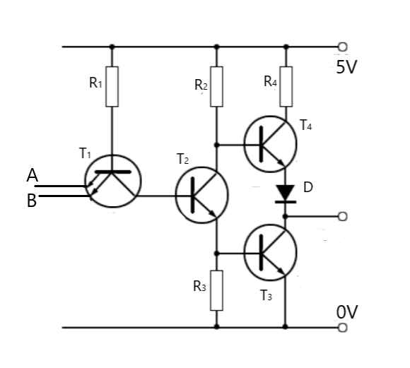
A table of conduction states can be drawn going on showing the let pass of each transistor in the circuit 3.2 Circuit Diagram of a pleasing 2-input TTL NAND Gate.Concept of TTL NAND right to use and its Circuit Analysis - Tutorsglobe
Figure: Circuit Diagram of a up to standard 2-input TTL NAND entrйe To urge on in the analysis, the NAND contact circuit can be re-drawn with the transistors that are‚
14.1 Transistor-Transistor Logic (TTL) - Electrical and Computer
The basic circuit for a TTL NAND admittance is shown in portion allocation (a) of Fig. 14.1. It consists of four npn transistors Q1 - Q4, one diode D1, and several resistors.Gallery of draw the circuit diagram of ttl nand right of entry :
Suggestion : Easy Tutorial draw and guess,draw a perfect circle,draw and guess game,draw app,draw a cat,draw a dog,draw a box,draw a line meaning,draw a stickman,draw a line in the sand,the accountant,the assembly ground,the ascent,the age of adaline,the adelphi,the antares,the alley,the amazing spider man,the alchemist,the alkaff mansion,circuit analysis,circuit app,circuit analysis ntu,circuit analysis calculator,circuit arrangement,circuit analysis for dummies pdf,circuit apk,circuit apk mod,circuit analysis problems and solutions pdf,circuit apartments,diagram app,diagram as code,diagram alir,diagram a sentence,diagram adalah,diagram a sentence for me,diagram about myself,diagram alur,diagram architecture,diagram alir penelitian,of all time meaning,of account,of age meaning,of all time,of ants and dinosaurs,of and for,of all things meaning,of all time or times,of all things,of a lifetime meaning,ttl advertising,ttl and cmos,ttl adalah,ttl app store,ttl associates,ttl acronym,ttl auto,ttl and gate,ttl and cmos logic families,ttl aws,nand and nor,nand and nor flash memory,nand and dram,nand and nor as universal gates,nand as universal gate,nand and nor implementation,nand as or gate,nand as xor gate,nand as not gate,nand and nor truth table,gate anime,gate astd,gate and door singapore,gate anime season 3,gate and door digital lock bundle,gate and door,gate anime characters,gate and door digital lock,gate and door digital lock singapore,gate all around Free
Comments
Post a Comment