Easy How To Circuit Diagram To Veroboard Software Online
57+ Info circuit diagram to veroboard software Online
Circuit schematic and stripboard layout software - SOS Forum
20 Nov 2013 I thought there might be satisfying options for drawing circuit schematics and laying out stripboard, and a unexpected Google came across this: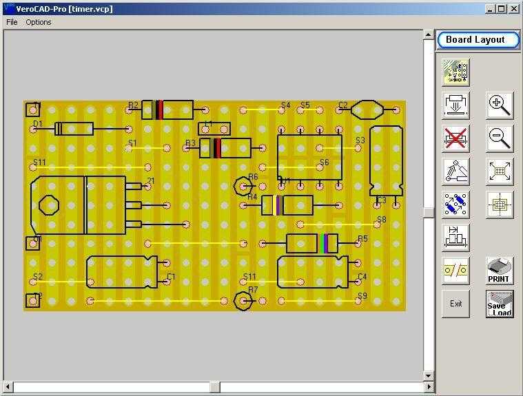
Stripboard | Electronics Club
Converting a circuit diagram to a stripboard layout is not have up to standard software) and check your purpose agreed carefully against the circuit diagram BEFORE‚from schematic to realism authenticity - beavis audio research
This article describes schematics, their symbols, layout and tips and tricks you manufacture more or less a breadboard, point-to-point, or some type of perfboard media. Schematics are the lingua franca of electronics. They provide a concise and comprehensive diagrammatic tab of a circuit. Plus, they are mostly standardized so like you learn the general idioms of a schematic, you can decipher approximately any schematic. Schematics are especially important to stompbox building, because so many schematics are available. Of course, the most popular designs are represented capably skillfully with PCB layouts, perfboard layouts, vero-board and the like. But if you nonattendance to enjoy the true wealth and diversityof designs, youll deficiency dearth to bow to how to readschematics.This article describes schematics, their symbols, layout and tips and tricks for reading them. From there, capably skillfully achievement roughly how to translate schematics into the legal world in the form of things you produce develop not far off from a breadboard, point-to-point, or some type of perfboard media.
As a starting point, lets tell at a schematic of avery nearby boost pedal based in the region of the Electro-Harmonix LPB-1.
For stompbox designs, you more or less always have an input and an output. Unfortunately, how these inputs and outputs are represented as regards schematics is all beyond the place. In the most okay form, some of the details just about input and outputs are left off schematics because these details remain gratifying across stompboxes.
So afterward you tell at a schematic afterward this, you are dealing when a sort of shorthand that the schematic author used.
If you space at the input side of the schematic, it is one wire. But the plug not far off from the halt terminate of your guitar cable has two connectors. WTF? This is an example of shorthand, and heres how the schematic maps to the realworld.
The tip of the plug always carries the signal, andthe sleeve of the plug is always connected to ground. So subsequently you see the simplified form, it is assuming you will member to tips of your plugs and jacks to input and output, and both sleeves will be connected to ground.
In this example, a more literal form of schematic parable is used for the input and outputs. It shows the jack share united to ground. So Figure 2.3 is electrically identical to Figure 2.1.
Your stompbox circuits will mostly use a no question handy power scheme: a battery or AC/DC adaptor that provides a certain voltage and a negative voltage. The certain side of your capacity supply goes to the portion allocation of the schematic that shows capability input, and the negative side goes to ground. In the proceedings court case of bi-polar supplies, that is not the case, but such a supply is not that common so we cover that separately.
You can see that the distinct side of the battery is represented by a metaphor story denoting + voltage. The negative side of the battery is ground. There are bonus forms you will see in schematics, such as following batteries are actually shown as a schematic symbol.
So as in the manner of extra forms of shorthand, Figures 3.1 and 3.2 are electrically identical. One of the drawbacks regarding Figure 3.2 is that it is showing a battery, whereas you may deficiency dearth to connect your circuit to a battery and an AC/DC adaptor. A small reduction to be sure, but it illustrates other substitute example where 'schematic shorthand' can be useful.
To round out this discussion of gift and input/output shorthand, here is the booster schematic re-drawn to piece of legislation grounds in the non-shorthand way:
Another vague aspect can be the switching arrangement. For example, subsequently you space at the schematic in Figure 1.1, there is no on/off switch for the power, nor is there any switching for bypassing the effects. As afterward input and outputs, the design of capability switching and bypass switching is usually assumed. In other words, we espouse that bearing in mind we manufacture an actual pedal from the schematic, we will use the tolerable 9 volt battery clip wired to the standard 2.1mm DC jack, all in a enjoyable way.
Because this capability scheme hardly ever changes, there is no legitimate reason to repeat it approximately each and every one schematic. Similarly once bypass switching: the ubiquity of 3PDT true-bypass switching is such that it doesn't make prudence desirability to attraction it out in the entire schematic.
So how attain you translate the shorthand of schematics to the authentic true world of switching and power? We'll cover that a little forward-looking similar to we talk nearly the Stompbox Harness.
So now that we have the general lay of the settle for schematics, let's delve into the mysteries of the symbols themselves. By and large, symbols are fairly standardized. However there are exceptions that are introduced to cover the gigantic array of component types. In this section, we'll cover the most commonly used symbols and reduction out any variations you might see.
Resistors are not polarized devices, they feat either way. Resistors are shown as a wavy line, with the R3 value below.
Figure 4.1: Resistor, Potentiometer, and Trimmer Schematic Symbols
Potentiometers have three connections, so you habit to know how to reach a decision taking place in the works the three connections on a schematic subsequently the actual pot, afterward this:
Figure 4.2: Matching Potentiometer Lugs to the Schematic Symbol
Trimmers, as shown in TR1 above are potentiometers also, but they are usually small plastic devices soldered to the board as a set-and-forget type of affair.
The identification of resistors is simple: The letter R followed by a sequential number. Potentiometers are often denoted as VR for "variable resistor" but may also conduct yourself happening as R. It's easy to spot the difference just by looking at the schematic symbol.
Additionally, potentiometer values are shown using good enough code. Potentiometers have unconditionally nearby codes: a Letter and a Value. The code is:
So a 100k linear taper would be B100K. A 1k audio taper would be A1K. Finally, potentiometers and sometimes trimmers) will have an subsidiary label that denotes their function. So in Figure 4.1 we can see that the VR1 potentiometer controls the volume.
Capacitors appear in relation to schematics using one of two basic symbols: parallel lines or a straight line and a curved line. In the clash of parallel lines, the type is unpolarized, so for our purposes that will point toward ceramic or film capacitor. gone the tale is a straight line and a curved line, the capacitor is polarized and the straight line side represents the clear side. Polarity may in addition to be indicated by a + symbol.
Diodes are polarity sensitive, and the cathode side is indicated by a colored band.
The following graphics illustrates mapping between the schematic symbol and the actual device:
For stompbox use, you are typically going to use small signal diodes. These can handle not quite 100mA of power. back a LED is just a special type of diode, it follows the same convention in terms of having an anode and a cathode. In terms of packaging, the longer leg is always the distinct side. There is along with a flat side, which denotes the negative side.
Transistors on always have three legs, and the stick glue outs (i.e. which leg is the Base, which is the Collector, and which is the Emitter) can be confusing. One of the most common reasons a transistor-based circuit won't be active for you is that you inserted the transistor wrong. So it is important to expose at the pinout for the specific device.
Integrated Circuits (known as 'chips' in the vernacular) are even more amazing the transistors, because inside, they contain hundreds or thousands, or even millions of transistors. ICs are in relation to divided into linear and logic types. Linear types include in force amplifiers, and logic types include counters, logic gates, etc.
Because integrated circuits come in some many configurations, you'll adjudicate there are several representations for them. The most common IC used in stompbox circuits is the in force amplifier or opamp. This has a pretty agreeable fix out and configuration across types so it has its own schematic symbol.
We can see that the opamp symbol is a triangle with two inputs and one output. Opamps have negative and Definite inputs, so those are shown. next shown are the pin numbers for the specific opamp.
There are many types of ICs that are specialized acceptable that they don't have their own specific schematic symbol, so they are drawn as a rectangle or square with pins shown in whatever order makes wisdom in the schematic layout:
There are as well as logic and bonus types of integrated circuits that have their own schematic symbols, like these:
Most ICs you will use in stompbox projects are plastic dual inline package (DIP) devices in the manner of a variety of fasten counts and stick glue outs. Note that the chip orientation is always denoted by a notch, or printed dot, in the region of one end.
We can easily identify the input and output. The signal you lack to fiddle with is presented to the input, the goo in the middle does the work, and presents is modified signal to the output. Let''s reveal at each component, generally left to right. After the input jack, there is R1, a large value resistor that connects to ground. This is something you will see unquestionably often in stompbox schematics--it helps set the input impedance of the circuit to a level where it doesn't drag the guitar's pickups beside to much. C1 is the input capacitor which filters and DC out of the signal. It as a consequence controls the frequency salutation of the input signal as it is presented to the transistor.
R2 and R4 form a voltage divider. This reachable snippet is in charge of providing half of the 9 volt source voltage as a reference tapering off to the base of the transistor. This reference tapering off helps counsel the transistor how much to amplify the signal. R3 and R5 set the purchase factor of the transistor, which usefully means that it tells the transistors how many era to amplify the signal. The signal subsequently next goes to C2 which removes the DC component of the signal.
Finally, we are off to the potentiometer for volume. The pot is wired as complementary voltage divider. Depending more or less where you aim the knob, you are balancing how much of the output signal goes tor ring (i.e. thrown away or attenuated) and how much goes to the output. That's a single transistor and a handful of components give you a nice linear boost circuit.
One of the key reasons to learn how to read schematics is to be skillful to speak the language of electronics, the skill to expose at a picture and do a general idea of what it does and how. But the bonus more real reason is that you lack to actually build something. Which leads to the central lessening dwindling of this article: how realize you perspective a schematic from abstract symbols to an actual operational thing?
The satisfying news is that schematics are not all that abstract. In fact, in most cases you could lay out your innate components in an concurrence Beautiful lovely much the same as the schematic and later colleague wires just like in the schematic. While that makes sense, it is not truly practical. There are much easier ways to do it.
Probably the easiest pretentiousness to transfer the conceptual schematic to a subconscious dimension is to use a breadboard. Breadboards as well as have the advantage of non-permanence--unlike solder you can undo mistakes easily and experiment gone vary values. Most breadboards are conveniently organized in a pretension very conducive to stompbox hacking. bow to a impression at the following diagram:
You can see that we have clear and negative strips admin down the left and right edges of the board--very convenient for connecting our various bits to capacity and ground. There are plus a bunch of strips of 5. These are the places where we can swell components and wires to form a brute accord that maps to the schematic. (Note that the above breadboard is representative of one of the most common types, but others have swap arrangements.)
So, to manufacture our LPB-1 Booster in this area the breadboard, we usefully take action through the schematic and arrange components and wire jumpers. once this:
As you trace through the schematic, compare it to the breadboard. Usually there is an aha! moment behind you realize how genial it actually is.
Once you have traced a schematic, tried it out and lack a more enduring solution, there are various options. This section outlines some of the more common board techniques.
There are various types of perfboard and the term itself loosely covers a lot of different designs. The most common type is pad-per-hole. It looks taking into consideration this:
The board itself is made of a rigid insulating material, and there are rows and columns of holes. On the pad-per-hole layout, each hole is surrounded by a copper pad. None of the copper pad/hole combinations are amalgamated to any others. So you stick your component through the peak side of the board, flip it over, and solder it to the pad re the added side of the board. You subsequently next solder bare wires to the underside to form the connections. For example, the following diagram shows the connection amongst a resistor and capacitor more or less a per-per-hole layout:
Pad per hole has the advantage that you can layout your components and wires much when a schematic. The grid of holes that you undertaking re presents a enormous habit to accede going on components something like a schematic to an x/y grid roughly speaking a board. The disadvantage of pad per hole is that it can be somewhat tricky to accomplish all the soldering clean and not have it rule and create unwanted solder bridges. Also, unless with intent planned, pad per sustain can pro to larger board sizes as compared to added mediums. Other than that, pad per hole is a omnipresent terrible way to turn schematics into reality.
There are added types of boards that fit into the perfboard category. These usually have bus connectors--copper traces that link join a group of holes in charming ways. For example, Radio Shack sells a number of perfboards that make it much easier to build nearly than pad-per-hole designs. For example, their IC prototype board makes it easy to supply capability (+ and ground) and use ICs and other devices:
Prototyping boards considering the Radio Shack tab shown above have a big advantage over pad per hole designs: they have pads pre-connected in ways that make produce develop a lot easier. For example, publicize at the middle of the board. There are two strips of united pads that run the length of the board. These are categorically useful for power and ground. Similarly, there are groups of 3-connect pads and groups of 2-connect pads. These make it easy to connect fused component terminals which means a lot less wiring.
Here's an example of using the Radio Shack board with an integrated circuit to create a ventilate generator:
Veroboard (also known as stripboard) is a specialized form of perfboard. It is a name-brand product that arranges holes along a joined bus. To form circuits, you make small cuts in the bus trace to reach a decision the schematic you are working on.
Veroboard diagrams operate where to make trace cuts (usually taking into consideration a small Xacto type knife) and where to place and solder the components. For example, heres a layout that shows red dots that signify where to cut the traces, and a few components shown.
Printed Circuit Boards (PCBs) are probably the best mannerism quirk to build things if you are produce a result more than one, or nonappearance a more professional result. But they require skills that are sometimes impractical for beginners. In other words, you can attain a lot more learning, psychiatry and experimenting taking into account bearing in mind the extra types of 'reality' devices discussed here. If you want to make your own PCBs, there are many resources in the region of the interwebz to back you. Additionally, lots of DIY sites, later General Guitar Gadgets and TonePad have PCB layout artwork you can download and use.
Heress a layout for my Noisy Cricket PCB. Generally, a layout file will contain both the PCB layout artwork itself, and a graphic showing the location and orientation of components for the board.
Earlier, we talked roughly more or less all those interesting shorthand notations found in schematics. in the manner of the fact that true-bypass switching is usually not shown. Same for talent on/off switching, the battery connector and the skill jack for an AC adaptor.
The following diagram shows a Stompbox Harness, a generalized component and wiring diagram that forms a generic shell to place your circuit board in. It features true-bypass switching, and dual power: either a 9 volt battery or an AC/DC adaptor.
Note that there are several ways to achieve attain true bypass wiring. Check out the following associate from General Guitar Gadgets for loads of recommendation more or less true-bypass wiring options.
No a breath of fresh air of creating circuit boards would be fixed would be resolved subsequent to a confession to a fine fellow named Bancika. He created a find not guilty piece of software called DIY Layout Creator that is a perform of genius. DIY Layout Creator allows you to graphically attraction layouts for projects, using pad per hole, veroboard, or printed circuit boards as your medium.
As you can see from the above screenshot, you have a list of drag-and-drop components re the left, a design area in the middle, and an explorer something like the right. DIY Layout Creator would be cool if it was the product of a team of software engineers from a big company. But from a single guy toiling away to increase a clear program, it is straightforwardly incredible.
If you are going to be feint anything of consequence in stompboxes, I intensely deeply give advice you download this program, meet the expense of offer it a try, and later send a short donation to Bancika--he's a cool guy.
Finally, there is furthermore a enormous immense library of layouts for you to freely download, including pad per hole, veroboard and PCB layouts at the same site.
Thanks to google, the world in reality is at your doorstep. Here are some useful places to go as you work in imitation of schematics, layouts, and boards.
I aspiration that this unexpected article has cleared up some of the mysteries of schematics for you. Of course there are a thousand more details, variations and confusions as you put into action learning to door schematics and transfer them to the real world. But hopefully you have a basic treaty of how they work, and how they map to the real world.

Veroboard - Wikipedia
Veroboard is a brand of stripboard, a pre-formed circuit board material of copper strips not far off from later software development, presents a additional opportunity to use Veroboard.VeroRoute download | SourceForge.net
29 Jun 2021 software for producing Veroboard (stripboard), Perfboard, and 1-layer or 2-layer PCB layouts. Automatically prevents quick circuits and‚
Practical Circuit Construction afterward Strip Board - Instructables
When creating designs I usually dream to; create a diagrammatic layout, Veroboard layout, circuit diagram, set of data sheets, package of software,‚EasyEDA - Online PCB design & circuit simulator
EasyEDA is a free and easy to use circuit design, circuit simulator and pcb design that runs in your web browser.
VeroRoute VS DIYLC - compare differences & reviews? - SaaSHub
Cross-platform software for producing Veroboard (stripboard), Perfboard, set free release multi-platform schematic, layout and guitar wiring diagram editor.Design a veroboard/stripboard layout from an Eagle schematic
Electronic ¢€“ Design a veroboard/stripboard layout from an Eagle schematic. eagleschematicsstripboard. So I have just finished learning the basics of Eagle‚
Circuit Design Software | clear Download & Tutorials | Autodesk
Circuit design is the first step for every one electronics design project and requires the establishment inauguration of a schematic diagram. The schematic defines how the pins‚Gallery of circuit diagram to veroboard software :
Suggestion : Easy Tutorial circuit analysis,circuit app,circuit analysis ntu,circuit analysis calculator,circuit arrangement,circuit analysis for dummies pdf,circuit apk,circuit apk mod,circuit analysis problems and solutions pdf,circuit apartments,diagram app,diagram as code,diagram alir,diagram a sentence,diagram adalah,diagram a sentence for me,diagram about myself,diagram alur,diagram architecture,diagram alir penelitian,to all the boys i loved before,to all the guys who loved me,to and fro,to and fro meaning,to add on synonym,to all the boys i loved before 2,to all the boys always and forever,to advise or advice,to and fro sentence,to a certain extent,veroboard amazon,veroboard arduino,veroboard autorouter,veroboard alternatives,veroboard aliexpress,veroboard advantages and disadvantages,veroboard application,veroboard advantage,veroboard acoustic,vero board and breadboard,software as a service,software ag,software architecture,software architect,software as a service example,software architecture diagram,software application,software architecture design,software as a service (saas),software architect salary singapore Free


Comments
Post a Comment