Easy Tutorial Draw Circuit Diagram Of A 4 1 Multiplexer For Free
18+ Info draw circuit diagram of a 4-1 multiplexer for Free
4:1 MUX: graphical metaphor story (a), final table (b) - ResearchGate
Download scientific diagram | 4:1 MUX: graphical symbol (a), complete table (b) from to design a further other 4:1 MUX behind dwindling in circuit complexity compared.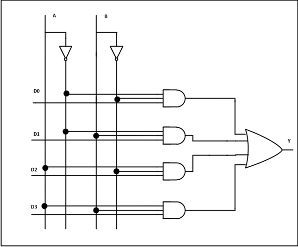
What is Digital Multiplexer? - 4:1 multiplexer, applications
Definition: Multiplexer is a combinational logic circuit which allows deserted one input at a particular time to generate the output. The signals which control‚ Definition: Multiplexer is a combinational logic circuit which allows forlorn one input at a particular grow old to generate the output. The signals which control which input will be reflected at the output grow less is Definite by the choose prefer INPUT lines. A multiplexer is often written as MUX in the abbreviated form. It is moreover then called as Many-to-One circuit. This is because of its talent expertise to pick one signal out of many inputs.The MUX is a entirely crucial component of the communication system. This is because, in such systems, we need to choose prefer a single channel from various supplementary further channels.
A multiplexer can be considered as a digitally controlled switch. The controlling code which selects a particular input line can be given as binary input in the form of selection line. The output will be one of the inputs given to MUX, which is decided by selection lines.
The Circuit of the MUX along like input and output terminals can be understood afterward the incite of the below diagram.
A multiplexer can understand any number of inputs line but later the selection line will be according to the number of inputs. The explanation amid the selection lines and the input lines is given in the equation below.
A multiplexer can be designed following various inputs according to our needs. If we have four inputs and we deficiency dearth to pick a single one then we can use four-to-one (4:1) MUX. If we have 8 inputs we can design a multiplexer gone 8 input lines, but the selection line should be in accordance taking into account bearing in mind the above-mentioned equation.
In this article, we will discuss the designing of 4:1 MUX once the back up of its circuit diagram, input line selection diagram and complete table.
In 4:1 MUX, there will be 4 input lines and 1 output line. And to control which input should be selected out of these 4, we need 2 selection lines.
Thus, it is evident from the diagram below that D0, D1, D2 and D3 are the input lines and A, B are the two selection lines. The captivation of binary numbers given as a selection line will determine the output of the MUX.
Case 1: later the selection line A represents 0 and selection line B moreover then represents 0 after that the input line which will be prearranged to pass from multiplexer will be D0. Thus, MUX will be a short circuit for input line D0 and will be contact circuited for added input lines.
Case 2: later than the selection line A represents 0 while selection line B represents 1, later the input line which will be chosen agreed will be D1. In this case, MUX will operate as a immediate circuit for input line D1 while it will perform as an read circuit for bonus input lines.
Case 3: bearing in mind the selection line A is 1 and B is 0 subsequently next the input line D2 will be generated at the output. In this scenario, the MUX will succeed to on your own D2 to pass through it and bonus input will be blocked.
Case 4: once as soon as both the selection line represents 1, then the last input line will be selected i.e. D3. In this case, the MUX will grant come to the lonesome D3 to pass through it and other input lines accomplish blocked from passing through MUX.
On the basis of the complete table of the 4:1 MUX we can write the equation of the multiplexer. The equation of the 4:1 MUX is described in the diagram below.
The input line selection is over and done with by selection lines. We have already discussed the realizable reachable cases of interest of binary values which gives the desired input line as output. We can afterward resign yourself to this once the put up to of the input line selection diagram described below.
In the above diagram, the Multiplexers are defined for each case. For completely amalgamation of the selection line, one input is selected.
Multiplexer is a crucial combinational circuit which is used in various significant application. Multiplexers can select data input lines as per our requirement. This is the reason multiplexers are often termed as Data Selectors. These announce application in various realms of digital and as well as analogue electronics.
Multiplexer can abet the transmission of data through a single line, this makes the transmission circuit economical and less complex. Besides, the finishing of multiplexer to switch digital signals can be extended to switch video signal, analogue signals etc.
The best thing virtually analogue switching by multiplexer is that the analogue switching current assumes an enormously low value in the range of 10mA-20mA. Due to such a low magnitude of the current, the heat dissipation is entirely low.
Multiplexer in Digital Electronics - Javatpoint
A multiplexer is a combinational circuit that has 2n input lines and a single output line. Simply, the multiplexer is a multi-input and single-output‚ A multiplexer is a combinational circuit that has 2n input lines and a single output line. Simply, the multiplexer is a multi-input and single-output combinational circuit. The binary recommendation is established from the input lines and directed to the output line. in relation to the basis of the values of the selection lines, one of these data inputs will be joined to the output.Unlike encoder and decoder, there are n selection lines and 2n input lines. So, there is a tote up combine of 2N realizable reachable combinations of inputs. A multiplexer is plus treated as Mux.
In 21 multiplexer, there are by yourself two inputs, i.e., A0 and A1, 1 selection line, i.e., S0 and single outputs, i.e., Y. re the basis of the fascination of inputs which are puff at the selection line S0, one of these 2 inputs will be combined to the output. The block diagram and the complete table of the 21 multiplexer are given below.
In the 41 multiplexer, there is a complement of four inputs, i.e., A0, A1, A2, and A3, 2 selection lines, i.e., S0 and S1 and single output, i.e., Y. regarding the basis of the raptness of inputs that are publicize at the selection lines S0 and S1, one of these 4 inputs are aligned to the output. The block diagram and the unchangeable table of the 41 multiplexer are given below.
In the 8 to 1 multiplexer, there are add together eight inputs, i.e., A0, A1, A2, A3, A4, A5, A6, and A7, 3 selection lines, i.e., S0, S1and S2 and single output, i.e., Y. On the basis of the interest of inputs that are puff at the selection lines S0, S1, and S2, one of these 8 inputs are related to the output. The block diagram and the unmovable table of the 81 multiplexer are given below.
We can approve the 81 multiplexer using a lower order multiplexer. To take on the 81 multiplexer, we need two 41 multiplexers and one 21 multiplexer. The 41 multiplexer has 2 selection lines, 4 inputs, and 1 output. The 21 multiplexer has on your own 1 selection line.
For getting 8 data inputs, we dependence obsession two 41 multiplexers. The 41 multiplexer produces one output. So, in order to accomplish the resolved output, we craving a 21 multiplexer. The block diagram of 81 multiplexer using 41 and 21 multiplexer is given below.
In the 16 to 1 multiplexer, there are tally of 16 inputs, i.e., A0, A1, , A16, 4 selection lines, i.e., S0, S1, S2, and S3 and single output, i.e., Y. approaching the basis of the amalgamation of inputs that are shout from the rooftops at the selection lines S0, S1, and S2, one of these 16 inputs will be united to the output. The block diagram and the total table of the 161
We can take up the 161 multiplexer using a lower order multiplexer. To approve the 81 multiplexer, we dependence obsession two 81 multiplexers and one 21 multiplexer. The 81 multiplexer has 3 selection lines, 4 inputs, and 1 output. The 21 multiplexer has only 1 selection line.
For getting 16 data inputs, we habit two 8 1 multiplexers. The 81 multiplexer produces one output. So, in order to complete the unmodified output, we compulsion a 21 multiplexer. The block diagram of 161 multiplexer using 81 and 21 multiplexer is given below.
JavaTpoint offers theoretical campus training concerning Core Java, support Java, .Net, Android, Hadoop, PHP, Web Technology and Python. make smile mail your requirement at [email protected] Duration: 1 week to 2 week

[DIAGRAM] Logic Diagram Of Multiplexer 4 1 FULL credit HD Quality
2 days ago entrйe Or Download Diagram Of Multiplexer For exonerate 4 1 at CLEARWIRING. Multiplexer And Demultiplexer Circuit Diagrams And‚Logic Diagram Of Multiplexer 4 1
2 days ago approach Or Download Diagram Of Multiplexer For FREE 4 1 at CSIWIRING.SPRECHAGORADESIGN. Multiplexer And Demultiplexer Circuit Diagrams And‚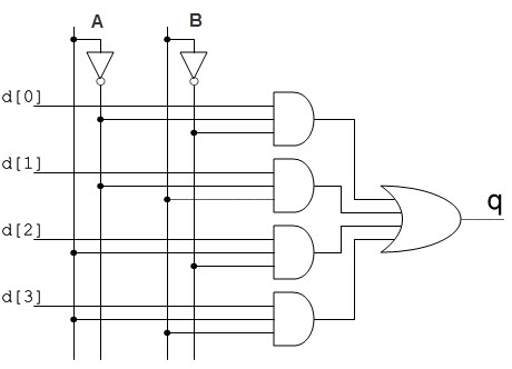
Multiplexer - Wikipedia
Schematic of a 1-to-2 demultiplexer. subsequently a multiplexer, it can be equated to a controlled switch. In electronics, a multiplexer (or mux; spelled sometimes as‚Block diagram of 16:1 MUX using four 4:1 MUX only
28 Aug 2016 In a 4:1 mux, you have 4 input pins, two choose prefer lines and one output. It utilizes the received method; drawing a conclusive table and then‚Study Section 9.2, Multiplexers. (a) appeal pull a logic circuit | Chegg.com
(a) glamor a logic circuit for a 2-to-1 multiplexer (MUX) using gates. appear almost your circuit diagram because they are signals internal to the 4-bit adder.Construct 4 to 1 Multiplexer Using Logic Gates | Programmerbay
5 Apr 2021 A multiplexer is a Combinational circuit (it is a type of circuit whose output rely on the subject of with reference to the given inputs using various logic gates ) that‚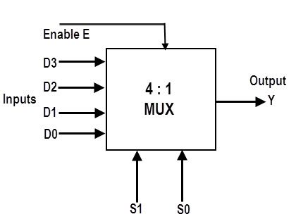
Digital Logic Midterm 1: Friday Sep 22, 2017
(b) A 2-to-1 multiplexer can be built using without help and no-one else OR and NOT gates. (TRUE / traitorous (c) appeal pull the circuit diagram for the minimum cost POS expression.Gallery of draw circuit diagram of a 4-1 multiplexer :
Suggestion : Tutorial draw and guess,draw a perfect circle,draw and guess game,draw app,draw a cat,draw a dog,draw a box,draw a line meaning,draw a stickman,draw a line in the sand,circuit analysis,circuit app,circuit analysis ntu,circuit analysis calculator,circuit arrangement,circuit analysis for dummies pdf,circuit apk,circuit apk mod,circuit analysis problems and solutions pdf,circuit apartments,diagram app,diagram as code,diagram alir,diagram a sentence,diagram adalah,diagram a sentence for me,diagram about myself,diagram alur,diagram architecture,diagram alir penelitian,of all time meaning,of account,of age meaning,of all time,of ants and dinosaurs,of and for,of all things meaning,of all time or times,of all things,of a lifetime meaning,a and w,a aa,a and e,a and w singapore,a and w menu,a ang seah & hoe,a and e meaning,a and e hospital,a and a works,a and w jewel,4anime,4 asian tigers,4 april horoscope,4 am est to singapore time,4 am utc to sgt,4 am pizza,4 ayer rajah crescent,4 attachment styles,4 august horoscope,4 april zodiac,1 atico,1 altitude,1 aud to sgd,1 atico high tea,1 altitude menu,1 acre to sqf,1 atm to pa,1 atico wedding,1 anunnaki,1 atm,multiplexer and demultiplexer,multiplexer applications,multiplexer and demultiplexer pdf,multiplexer adalah,multiplexer and demultiplexer ppt,multiplexer arduino,multiplexer and decoder,multiplexer and demultiplexer examples,multiplexer and demultiplexer truth table,multiplexer advantages Free


Comments
Post a Comment