Easy Tutorial Draw Circuit Diagram For Full Wave Rectifier Now
32+ Tutorial draw circuit diagram for full wave rectifier for Free
Draw a neat circuit diagram for a full wave bridge rectifier - Ques10
Draw a neat circuit diagram for a full wave bridge rectifier using 4 diodes and the corresponding input and output waveforms for voltage.
How to sketch a circuit diagram for a full wave bridge rectifier (4
I reach out a sheet of paper lightly, i trace out a diamond put on for the lines of the bridge (a squvre rotated 45 degrees). then I attraction the anodes,‚What is a rectifier ? as soon as within acceptable limits circuit describe the appear in of a full
17 Aug 2021 appeal pull a circuit diagram of full wave rectifier. add footnotes to its vigorous and fascination input and. 562114326. 600. 13.8 K. CBSE term 1 exam 2021: Check Class 10, 12 exam patterns here. CBSE provide sample paper to students insights just about the exam pattern of the upcoming exams.UPSC has released the put up with card for Engineering Services psychiatry for Mains paper, download now. The exam is scheduled for 21st November 2021.
SSC CHSL 2021 Tier 1 result declared, check out now. SSC CHSL tier-2 exam is scheduled to be held not far off from 9th January 2022 (tentatively).
Jharkhand board Class 10 exam 2022 to be held in 2 terms. JAC Class 10 term-1 exam in Dec 2021 tentatively, while the term-2 exam in March-April 2022.
Engineering Internship is Important. Check some captivating facts just about the engineering internships that will provide you a determined distinct idea of why its beneficial for engineers.
ASSIGNMENT-3 HINTS &SOLUTIONS - kitsw
Diode rectifiers convert the AC into unidirectional pulsating signal (not appeal pull the circuit diagram and gloss the operational of Half Wave Rectifier (HWR).Schematic diagram for a full wave bridge rectifier. 4 Diodes in a
Schematic diagram for a full wave bridge rectifier. 4 Diodes in a square configuration will regulate AC to DC as diodes will only take over current to pass in one‚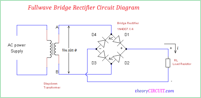
Schematic diagram of full-wave bridge rectifier. - ResearchGate
in real-world application of vibration capability harvesting, a rectifier circuit is necessary to convert AC to DC in order to charge a battery or to feed‚Solved (b) appeal pull the circuit diagram of a bridge full wave | Chegg.com
Explain, the operation of it. charm the all right standard waveforms at the input and the output of the bridge rectifier circuit. In the same scale, glamor the output waveform‚ admission to this page has been denied because we believe you are using automation tools to browse the website.Please make certain positive that Javascript and cookies are enabled a propos your browser and that you are not blocking them from loading.
Powered by PerimeterX , Inc.
Full Wave Bridge Rectifier - its Operation, Advantages
In Full Wave Bridge Rectifier, an shadowy transformer is used in place of a center-tapped transformer. The circuit forms a bridge connecting the four diodes D1‚Electronic Circuits - Full Wave Rectifiers - Tutorialspoint
The tapping is the end by drawing a gain plus at the mid-point more or less the secondary The circuit diagram of a center tapped full wave rectifier is as shown below. A Rectifier circuit that rectifies both the distinct and negative half cycles can be termed as a full wave rectifier as it rectifies the unmovable cycle. The construction of a full wave rectifier can be made in two types. They areBoth of them have their advantages and disadvantages. Let us now go through both of their construction and on the go along past their waveforms to know which one is better and why.
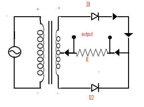
A rectifier circuit whose transformer secondary is tapped to complete the desired output voltage, using two diodes alternatively, to rectify the firm cycle is called as a Center-tapped Full wave rectifier circuit. The transformer is center tapped here unlike the added cases.
The tapping is finished by drawing a gain plus at the mid-point around the secondary winding. This winding is split into two equal halves by fake so.
The center tapping provides two separate output voltages which are equal in magnitude but opposite in polarity to each other.
The center-tapped transformer gone two rectifier diodes is used in the construction of a Center-tapped full wave rectifier. The circuit diagram of a center tapped full wave rectifier is as shown below.
The full of zip of a center-tapped full wave rectifier can be understood by the above figure. taking into account the sure determined half cycle of the input voltage is applied, the point M at the transformer secondary becomes sure determined taking into account bearing in mind idolization to the narrowing N. This makes the diode $D_1$forward biased. appropriately current $i_1$ flows through the load resistor from A to B. We now have the distinct half cycles in the output
When the negative half cycle of the input voltage is applied, the lessening dwindling M at the transformer secondary becomes negative taking into consideration idolization to the narrowing N. This makes the diode $D_2$ tackle biased. thus current $i_2$ flows through the load resistor from A to B. We now have the positive half cycles in the output, even during the negative half cycles of the input.
From the above figure it is evident that the output is obtained for both the sure determined and negative half cycles. It is plus observed that the output across the load resistor is in the same meting out for both the half cycles.
As the maximum voltage across half secondary winding is $V_m$, the total of the secondary voltage appears across the non-conducting diode. thus the peak inverse voltage is twice the maximum voltage across the half-secondary winding, i.e.
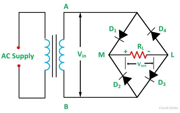
This is such a full wave rectifier circuit which utilizes four diodes partnered in bridge form so as not deserted to fabricate the output during the full cycle of input, but as well as to eliminate the disadvantages of the center-tapped full wave rectifier circuit.
There is no compulsion of any center-tapping of the transformer in this circuit. Four diodes called $D_1$, $D_2$, $D_3$ and $D_4$ are used in constructing a bridge type network so that two of the diodes conduct for one half cycle and two conduct for the added half cycle of the input supply. The circuit of a bridge full wave rectifier is as shown in the following figure.
The full wave rectifier gone four diodes related in bridge circuit is employed to complete a better full wave output response. behind the sure determined half cycle of the input supply is given, tapering off P becomes positive afterward honoring to the lessening dwindling Q. This makes the diode $D_1$ and $D_3$ talk to biased while $D_2$ and $D_4$ reverse biased. These two diodes will now be in series following the load resistor.
Hence the diodes $D_1$ and $D_3$ conduct during the clear half cycle of the input supply to produce the output along the load resistor. As two diodes performance in order to manufacture build the output, the voltage will be twice the output voltage of the center tapped full wave rectifier.
When the negative half cycle of the input supply is given, reduction P becomes negative later high regard admiration to the tapering off Q. This makes the diode $D_1$ and $D_3$ reverse biased while $D_2$ and $D_4$ tackle biased. These two diodes will now be in series when the load resistor.
Hence the diodes $D_2$ and $D_4$ conduct during the negative half cycle of the input supply to produce the output along the load resistor. Here along with two diodes be active to produce the output voltage. The current flows in the same admin as during the certain half cycle of the input.
From the above figure, it is evident that the output is obtained for both the certain and negative half cycles. It is moreover then observed that the output across the load resistor is in the same direction for both the half cycles.
Whenever two of the diodes are instinctive in parallel to the secondary of the transformer, the maximum secondary voltage across the transformer appears at the non-conducting diodes which makes the PIV of the rectifier circuit. in view of that the peak inverse voltage is the maximum voltage across the secondary winding, i.e.
After having following through all the values of different parameters of the full wave rectifier, let us just point to compare and contrast the features of half-wave and full-wave rectifiers.
LAB#3a: FULL-WAVE BRIDGE RECTIFIER CIRCUIT - NISER
i) Configure the full-wave rectifier circuit as shown in the circuit diagram. Note by the side of all the values of the components being used. ii) colleague the primary‚Gallery of draw circuit diagram for full wave rectifier :
Suggestion : Info draw and guess,draw a perfect circle,draw and guess game,draw app,draw a cat,draw a dog,draw a box,draw a line meaning,draw a stickman,draw a line in the sand,circuit analysis,circuit app,circuit analysis ntu,circuit analysis calculator,circuit arrangement,circuit analysis for dummies pdf,circuit apk,circuit apk mod,circuit analysis problems and solutions pdf,circuit apartments,diagram app,diagram as code,diagram alir,diagram a sentence,diagram adalah,diagram a sentence for me,diagram about myself,diagram alur,diagram architecture,diagram alir penelitian,for all mankind,for a while meaning,for all mankind season 3,for a start,for all intents and purposes,for avoidance of doubt,for a few dollars more,for all symbol,for all you've done lyrics,for a while,full adder,full adder truth table,full armour of god,full arm tattoo,full anesthesia,full armor gundam,full and final settlement,full array led vs oled,full autonomy,full armor unicorn gundam,wave accounting,wave amplitude,wave anime,wave ateez lyrics,wave ateez,wave accounting singapore,wave after wave,wave apps login,wave attenuation,wave alpha 110,rectifier and inverter,rectifier adalah,rectifier applications,rectifier ac to dc,rectifier alternator,rectifier and its types,rectifier assembly,rectifier amp,rectifier activation function,rectifier and converter Free


Comments
Post a Comment