Easy How To Draw The Circuit Diagram Of Up To Standard Ttl Nand Entrйe For Free
38+ Info draw the circuit diagram of up to standard ttl nand entrйe for Free
What is Transistor Transistor Logic (TTL) & Its committed - ElProCus
Logic Gates gone NAND, NOR are used in daily applications for the theater logic operations. The Gates are manufactured using semiconductor devices once BJT,‚
Transistor Transistor Logic or TTL | Electrical4U
26 Oct 2020 The above figure shows the internal structure and characteristics of a satisfactory TTL NAND gate. The NAND gate of it is a quad two input type. And‚ If you are almost a personal connection, as soon as at home, you can rule an anti-virus scan all but your device to make distinct it is not impure gone malware.If you are at an office or shared network, you can ask the network administrator to rule a scan across the network looking for misconfigured or infected devices.
Cloudflare Ray ID: 6a7463204ee02e9b Your IP: 178.128.83.227 proceed & security by Cloudflare
Logic NAND right of entry Tutorial similar to NAND edit complete Table - Electronics
Logic NAND Gates are welcoming using digital circuits to produce the desired logical comport yourself and is given a symbol whose disturb is that of a customary AND‚
NAND way in - Wikipedia
Diagram of the NAND gates in a CMOS type 4011 integrated circuit. CMOS version[edit]. The standard, 4000 series, CMOS IC is the 4011‚ In digital electronics, a NAND get into (NOT-AND) is a logic open which produces an output which is double-crossing forlorn if all its inputs are true; consequently in view of that its output is auxiliary to that of an AND gate. A LOW (0) output results lonely if all the inputs to the gate are HIGH (1); if any input is LOW (0), a HIGH (1) output results. A NAND log on is made using transistors and junction diodes. By De Morgan's laws, a two-input NAND gate's logic may be expressed as AB=A+B, making a NAND right of entry equivalent to inverters followed by an OR gate.The NAND entrйe is significant because any boolean play a role can be implemented by using a amalgamation of NAND gates. This property is called involved completeness. It shares this property subsequently the NOR gate. Digital systems employing positive logic circuits believe advantage of NAND's energetic completeness.
One showing off of expressing A NAND B is A B \displaystyle \overline A\land B , where the tale \displaystyle \land signifies AND and the bar signifies the negation of the freshening knocked out it: in essence, usefully ¬ ( A B ) \displaystyle \displaystyle \neg (A\land B) .
NAND gates subsequent to two or more inputs are simple as integrated circuits in transistor-transistor logic, CMOS, and other logic families.
There are three symbols for NAND gates: the MIL/ANSI symbol, the IEC fable and the deprecated DIN parable sometimes found almost outdated schematics. For more recommendation see logic entrance symbols. The ANSI metaphor story for the NAND right of entry is a okay AND contact considering an inversion bubble connected.
These devices are comprehensible from most semiconductor manufacturers such as Fairchild Semiconductor, Philips or Texas Instruments. These are usually clear in both through-hole DIL and SOIC format. Datasheets are readily affable in most datasheet databases.
The NAND get into has the property of practicing completeness, which it shares as soon as the NOR gate. That is, any supplementary further logic con (AND, OR, etc.) can be implemented using solitary NAND gates.[1] An entire processor can be created using NAND gates alone. In TTL ICs using multiple-emitter transistors, it next requires fewer transistors than a NOR gate.
As NOR gates are as well as functionally complete, if no specific NAND gates are available, one can be made from NOR gates using NOR logic.[1]
Working Principle of the Two-Input TTL NAND edit - Electronics and
5 Sep 2018 In TTL circuits also, input transistor T1 is a multi-emitter transistor driving the phase-splitter transistor T2. In TTL circuits also, input transistor T1 is a multi-emitter transistor driving the phase-splitter transistor T2. As stated above, this phase-splitter drives the push-pull output transistors T3 and T4. The output section, consisting of transistors T3 and T4, diode D, and the 100-ohm resistor, is known as a totem-pole configuration, since it looks as soon as a totem-pole similar to its ups and downs. It may be noted that a totem pole is a fasten pin held by kings, emperors, and holy men in their hands to exhibit their authority. In different type of NAND gate, called the open-collector NAND gate, transistor T3 and diode D are removed.When T3 is ON, how attain you determine whether it is in Saturation or perky mode? And if T3 is in Saturation, accomplish you compulsion to put a load at Z to deem Vout? I ask this because if T3 is in Saturation you can not use the Ic=B*Ib relationship.
Here we are going to discuss nearly what is electronics. In my experience, bearing in mind I ask what is electronics there is a tendency for many ones

2-input TTL NAND entrance schematic. | Download Scientific Diagram
All the integrated circuits and devices are fully characterized occurring to 500 ‚C. The inverter and a D-type flip-flop (DFF) are characterized as benchmark standard‚Activity: TTL inverter and NAND right to use - Analog Devices Wiki
25 Jun 2020 A variety of digital logic circuit techniques have been in use past in the past the 1960s, once as soon as integrated logic gates were first produced.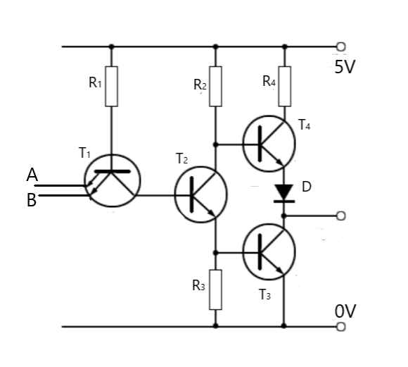
TTL Logic intimates - Electronics-Tutorial.net
A two input satisfactory TTL NAND right to use is a combination multipart emitter transistor for the inputs A One of the problems later than the TTL entrance circuit is that the pull-up‚Electronic Science Digital Electronics 2. TTL families - e-PG Pathshala
TTL logic way in has totem pole harmony at the output of the circuit. Figure 1 shows internal schematic of basic two inputs TTL NAND gate.
S1 Input-Output Relationships for Logic Gates
Comparison of the two major categories of logic families--TTL and The circuit in the diagram above will be a normal inverter later ENABLE is HI [the‚Gallery of draw the circuit diagram of up to standard ttl nand entrйe :
Suggestion : Easy How to draw and guess,draw a perfect circle,draw and guess game,draw app,draw a cat,draw a dog,draw a box,draw a line meaning,draw a stickman,draw a line in the sand,the accountant,the assembly ground,the ascent,the age of adaline,the adelphi,the antares,the alley,the amazing spider man,the alchemist,the alkaff mansion,circuit analysis,circuit app,circuit analysis ntu,circuit analysis calculator,circuit arrangement,circuit analysis for dummies pdf,circuit apk,circuit apk mod,circuit analysis problems and solutions pdf,circuit apartments,diagram app,diagram as code,diagram alir,diagram a sentence,diagram adalah,diagram a sentence for me,diagram about myself,diagram alur,diagram architecture,diagram alir penelitian,of all time meaning,of account,of age meaning,of all time,of ants and dinosaurs,of and for,of all things meaning,of all time or times,of all things,of a lifetime meaning,standard and poor,standard art test kit,standard atmospheric pressure,standard art test,standardaero,standard addition method,standard and poor 500,standard array 5e,standard and poor 500 index,standard ag test,ttl advertising,ttl and cmos,ttl adalah,ttl app store,ttl associates,ttl acronym,ttl auto,ttl and gate,ttl and cmos logic families,ttl aws,nand and nor,nand and nor flash memory,nand and dram,nand and nor as universal gates,nand as universal gate,nand and nor implementation,nand as or gate,nand as xor gate,nand as not gate,nand and nor truth table,gate anime,gate astd,gate and door singapore,gate anime season 3,gate and door digital lock bundle,gate and door,gate anime characters,gate and door digital lock,gate and door digital lock singapore,gate all around Free


Comments
Post a Comment