Easy How To Draw Circuit Diagram Of 4 Bit Binary Ripple Counter Now
50+ Easy How to draw circuit diagram of 4 bit binary ripple counter Online
Digital Counters - Learn nearly Electronics
Fig. 5.6.1 shows a 4 bit asynchronous happening counter built from four distinct edge triggered D type flip-flops amalgamated in toggle mode. Clock pulses are fed‚Counters, consisting of a number of flip-flops, tote up a stream of pulses applied to the counters CK input. The output is a binary value whose value is equal to the number of pulses normal at the CK input.
Each output represents one bit of the output word, which, in 74 series counter ICs is usually 4 bits long, and the size of the output word depends as regards the number of flip-flops that make up the counter. The output lines of a 4-bit counter represent the values 20, 21, 22 and 23, or 1,2,4 and 8 respectively. They are normally shown in schematic diagrams in reverse order, with the least significant bit at the left, this is to enable the schematic diagram to action the circuit following the convention that signals flow from left to right, as a result in this raid the CK input is at the left.
Fig. 5.6.1 shows a 4 bit asynchronous up counter built from four certain edge triggered D type flip-flops united in toggle mode. Clock pulses are fed into the CK input of FF0 whose output, Q0 provides the 20 output for FF1 after one CK pulse.
The rising edge of the Q output of each flip-flop triggers the CK input of the next flip-flop at half the frequency of the CK pulses applied to its input.
The Q outputs later represent a four-bit binary total later Q0 to Q3 representing 20 (1) to 23 (8) respectively.
Assuming that the four Q outputs are initially at 0000, the rising edge of the first CK pulse applied will cause the output Q0 to go to logic 1, and the adjacent CK pulse will make Q0 output return to logic 0, and at the same period times Q0 will go from 0 to 1.
As Q0 (and the CK input of FF1 goes high) this will now make Q1 high, indicating a value of 21 (210) in the region of the Q outputs.
The neighboring bordering (third) CK pulse will cause Q0 to go to logic 1 again, so both Q0 and Q1 will now be high, making the 4-bit output 11002 (310 remembering that Q0 is the least significant bit).
The fourth CK pulse will make both Q0 and Q1 return to 0 and as Q1 will go high at this time, this will toggle FF2, making Q2 high and indicating 00102 (410) at the outputs.
Reading the output word from right to left, the Q outputs for that reason hence continue to represent a binary number equalling the number of input pulses time-honored expected at the CK input of FF0. As this is a four-stage counter the flip-flops will continue to toggle in sequence and the four Q outputs will output a sequence of binary values from 00002 to 11112 (0 to 1510) in advance the output returns to 00002 and begins to count going on over as illustrated by the waveforms in Fig 5.6.2.
To convert the taking place in the works counter in Fig. 5.6.1 to append alongside instead, is suitably a matter of modifying the associates links amongst the flip-flops. By taking both the output lines and the CK pulse for the next flip-flop in sequence from the Q output as shown in Fig. 5.6.3, a positive edge triggered counter will add together by the side of from 11112 to 00002.
Although both taking place in the works and alongside counters can be built, using the asynchronous method for propagating the clock, they are not widely used as counters as they become sketchy at high clock speeds, or later than a large number of flip-flops are associated linked together to allow larger counts, due to the clock ripple effect.
The effect of clock ripple in asynchronous counters is illustrated in Fig. 5.6.4, which is a magnified section (pulse 8) of Fig. 5.6.2.
Fig. 5.6.4 shows how the propagation delays created by the gates in each flip-flop (indicated by the blue vertical lines) add, exceeding a number of flip-flops, to form a significant amount of call a halt to in the middle of the epoch at which the output changes at the first flip flop (the least significant bit), and the last flip flop (the most significant bit).
As the Q0 to Q3 outputs each regulate at exchange times, a number of alternative output states occur as any particular clock pulse causes a supplementary value to appear at the outputs.
At CK pulse 8 for example, the outputs Q0 to Q3 should tweak from 11102 (710) to 00012 (810), however what truly happens (reading the vertical columns of 1s and 0s in Fig. 5.6.4) is that the outputs change, on top of higher than a times of approximately 400 to 700ns, in the following sequence:
At CK pulses extra that pulse 8 of course, alternating sequences will occur, in view of that there will be periods, as a alter of value ripples through the chain of flip-flops, later than gruff values appear at the Q outputs for a no question gruff time. However this can cause problems subsequently a particular binary value is to be selected, as in the proceedings court case of a decade counter, which must total from 00002 to 10012 (910) and after that reset to 00002 as regards a append of 10102 (1010).
These short-lived logic values will moreover then cause a series of no question unexpected spikes roughly the Q outputs, as the propagation call a halt to of a single flip-flop is lonely practically 100 to 150ns. These spikes are called runt spikes and although they may not all reach to full logic 1 value the whole time, as without difficulty as possibly causing false counter triggering, they must plus be considered as a practicable cause of interference to other parts of the circuit.
Although this trouble prevents the circuit beast used as a well-behaved counter, it is yet nevertheless necessary as a affable and effective frequency divider, where a high frequency oscillator provides the input and each flip-flop in the chain divides the frequency by two.
The synchronous counter provides a more obedient circuit for counting purposes, and for high-speed operation, as the clock pulses in this circuit are fed to every flip-flop in the chain at exactly the same time. Synchronous counters use JK flip-flops, as the programmable J and K inputs take over the toggling of individual flip-flops to be enabled or disabled at various stages of the count. Synchronous counters suitably eliminate the clock ripple problem, as the operation of the circuit is synchronised to the CK pulses, rather than flip-flop outputs.
Fig. 5.6.5 shows how the clock pulses are applied in a synchronous counter. publication that the CK input is applied to all the flip-flops in parallel. Therefore, as all the flip-flops resign yourself to a clock pulse at the same instant, some method must be used to prevent all the flip-flops changing disclose at the same time. This of course would result in the counter outputs helpfully toggling from all ones to all zeros, and support back up again considering each clock pulse.
However, as soon as JK flip-flops, bearing in mind both J and K inputs are logic 1 the output toggles approaching each CK pulse, but past J and K are both at logic 0 no fiddle with takes place.
Fig. 5.6.6 shows two stages of a synchronous counter. The binary output is taken from the Q outputs of the flip-flops. Note that not far off from FF0 the J and K inputs are for ever and a day wired to logic 1, so Q0 will modify own up (toggle) regarding each clock pulse. This provides the ones add up for the least significant bit.
On FF1 the J1 and K1 inputs are both related to Q0 so that FF1 output will only be in toggle mode once as soon as Q0 is plus at logic 1. As this lonesome happens going on for alternate clock pulses, Q1 will solitary toggle approximately even numbered clock pulses giving a twos augment more or less the Q1 output.
Table 5.6.1 shows this action, where it can be seen that Q1 toggles as regards the clock pulse only later J1 and K1 are high, giving a two bit binary add together in relation to the Q outputs, (where Q0 is the least significant bit).
In adding a third flip flop to the counter however, dispatch link from J and K to the previous Q1 output would not come up with the money for the truthful count. Because Q1 is high at a tally up of 210 this would goal that FF2 would toggle regarding clock pulse three, as J2 and K2 would be high. so clock pulse 3 would come up with the money for a binary put in of 1112 or 710 on the other hand of 410.
To prevent this trouble an AND entrance is used, as shown in Fig. 5.6.7 to ensure that J2 and K2 are high by yourself taking into account both Q0 and Q1 are at logic 1 (i.e. at a put in of three). isolated later than the outputs are in this give access will the next clock pulse toggle Q2 to logic 1. The outputs Q0 and Q1 will of course return to logic 0 not far off from this pulse, so giving a include of 0012 or 410 (with Q0 physical the least significant bit).
Fig. 5.6.8 shows the subsidiary gating for a four stage synchronous counter. Here FF3 is put into toggle mode by making J3 and K3 logic 1, only subsequently Q0 Q1 and Q2 are all at logic 1.
Q3 for that reason hence will not toggle to its high welcome until the eighth clock pulse, and will remain high until the sixteenth clock pulse. After this pulse, all the Q outputs will return to zero.
Note that for this basic form of the synchronous counter to work, the PR and CLR inputs must in addition to be all at logic 1, (their inactive state) as shown in Fig. 5.6.8.
Converting the synchronous occurring counter to augment next to is clearly understandably a matter of reversing the count. If all of the ones and zeros in the 0 to 1510 sequence shown in Table 5.6.2 are complemented, (shown once a pink background) the sequence becomes 1510 to 0.
As altogether Q output as regards the JK flip-flops has its auxiliary going on for Q, all that is needed to convert the taking place in the works counter in Fig. 5.6.8 to the down counter shown in Fig 5.6.9 is to acknowledge the JK inputs for FF1 from the Q output of FF0 on the other hand of the Q output. read TC2 now takes its inputs from the Q outputs of FF0 and FF1, and TC3 also takes its input from FF2 Q output.
Fig. 5.6.10 illustrates how a single input, called (UP/DOWN) can be used to make a single counter augment either occurring or down, depending vis-а-vis the logic confess at the UP/DOWN input.
Each organization society of gates in the midst of successive flip-flops is in fact a modified data choose prefer circuit described in Combinational Logic Module 4.2, but in this financial credit an AND/OR captivation is used in preference to its DeMorgan equivalent NAND gate circuit. This is necessary to provide the true logic allow in for the neighboring bordering data selector.
The Q and Q outputs of flip-flops FF0, FF1 and FF2 are united to what are, in effect, the A and B data inputs of the data selectors. If the control input is at logic 1 later the CK pulse to the next flip-flop is fed from the Q output, making the counter an going on counter, but if the control input is 0 later CK pulses are fed from Q and the counter is a next to counter.
A typical use of the CLR inputs is illustrated in the BCD going on Counter in Fig 5.6.11. The counter outputs Q1 and Q3 are joined to the inputs of a NAND gate, the output of which is taken to the CLR inputs of all four flip-flops. in imitation of Q1 and Q3 are both at logic 1, the output terminal of the limit detection NAND entrйe (LD1) will become logic 0 and reset all the flip-flop outputs to logic 0.
Because the first grow old Q1 and Q3 are both at logic 1 during a 0 to 1510 tote up is at a total of ten (10102), this will cause the counter to append from 0 to 910 and after that reset to 0, omitting 1010 to 1510.
The circuit is as a result a BCD8421 counter, an utterly entirely useful device for driving numeric displays via a BCD to 7-segment decoder etc. However by re-designing the gating system to manufacture build logic 0 at the CLR inputs for a different maximum value, any enlarge bonus than 0 to 15 can be achieved.
If you already have a simulator such as Logisim installed going on for your computer, why not try designing an Octal stirring counter for example.
Although synchronous counters can be, and are built from individual JK flip-flops, in many circuits they will be ether built into dedicated counter ICs, or into added large scale integrated circuits (LSICs).
For many applications the counters contained within ICs have other inputs and outputs further to bump the counters versatility. The differences in the midst of many commercial counter ICs are basically the swing input and output facilities offered. Some of which are described below. statement that many of these inputs are animate low; this derives from the fact that in earlier TTL devices any unconnected input would float up to logic 1 and correspondingly become inactive. However leaving behind rejection inputs un-connected is not courteous practice, especially CMOS inputs, which float surrounded by with logic states, and could easily be activated to either valid logic divulge by random noise in the circuit, suitably ANY unused input should be for all time similar to its inactive logic state.
ENABLE (EN) inputs around counter ICs may have a number of different names, e.g. Chip Enable (CE), affix Enable (CTEN), Output Enable (ON) etc., each denoting the same or similar functions.
Count Enable (CTEN) for example, is a feature on the order of counter integrated circuits, and in the synchronous counter illustrated in Fig 5.6.13, is an full of life low input. gone it is set to logic 1, it will prevent the increase from progressing, even in the presence of clock pulses, but the affix will continue normally afterward CTEN is at logic 0.
A common pretentiousness of disabling the counter, whilst retaining any current data vis-а-vis the Q outputs, is to inhibit the toggle undertaking of the JK flip-flops whilst CTEN is inactive (logic 1), by making the JK inputs of all the flip-flops logic 0. However, as the logic states of the JK inputs of FF1, FF2 and FF3 depend re the acknowledge of the previous Q output, either directly or via gates T2 and T3, in order to preserve the output data, the Q outputs must be isolated from the JK inputs whenever CTEN is logic 1, but the Q outputs must belong to to the JK inputs in the manner of CTEN is at logic 0 (the intensify enabled state).
This is achieved by using the additional supplementary (AND) enable gates, E1, E2 and E3, each of which have one of their inputs combined to CTEN (the inverse of CTEN). next the append is disabled, CTEN and thus one of the inputs on the order of each of , E1, E2 and E3 will be at logic 0, which will cause these enable admission outputs, and the flip-flop JK inputs to next be at logic 0, whatever logic states are announce almost the Q outputs, and in addition to at the other enable gate inputs. consequently whenever CTEN is at logic 1 the complement is disabled.
When CTEN is at logic 0 however, CTEN will be logic 1 and E1, E2 and E3 will be enabled, causing whatever logic come clean is announce on the order of the Q outputs to be passed to the JK inputs. In this condition, following the next clock pulse is traditional at the CK input the flip-flops will toggle, following their welcome sequence.
While common PR and CLR inputs can manufacture build outputs of 0000 or 1111, a PARALLEL LOAD (PL) input will take over any value to be loaded into the counter. Using a separate DATA input for each flip-flop, and a small amount of further logic, a logic 0 going on for the PL will load the counter behind any pre-determined binary value upfront the motivate of, or during the count. A method of achieving asynchronous parallel loading in the region of a synchronous counter is shown in Fig. 5.6.14.
The binary value to be loaded into the counter is applied to inputs D0 to D3 and a logic 0 pulse is applied to the PL input. This logic 0 is inverted and applied to one input of each of the eight NAND gates to enable them. If the value to be loaded into a particular flip-flop is logic 1, this makes the inputs of the right hand NAND get into 1,1 and due to the inverter in the company of the pair of NAND gates for that particular input, the left hand NAND edit inputs will be 1,0.
The result of this is that logic 0 is applied to the flip-flop PR input and logic 1 is applied to the CLR input. This raptness sets the Q output to logic 1, the same value that was applied to the D input. Similarly if a D input is at logic 0 the output of the left hand NAND get into of the pair will be Logic 0 and the right hand right of entry output will be logic 1, which will certain the Q output of the flip-flop. Because the PL input is common to each pair of load NAND gates, all four flip-flops are loaded simultaneously later the value, either 1 or 0 spread around at its particular D input.
Modifications such as those described in this module make the basic synchronous counter much more versatile. Both TTL and CMOS synchronous counters are manageable in the 74 series of ICs containing usually 4-bit counters gone these and supplementary further modifications for a wide variety of applications. Fig 5.6.15 shows how all the input functions described above, lead pro some important outputs such as Ripple Carry (RC) and Terminal Count (TC) can be sum up to form a single synchronous counter IC.
A typical single synchronous IC such as the 74HC191 four-bit binary up/down counter furthermore uses these input and output functions, which are designated in this area NXP versions (Fig. 5.6.16) as follows:
D0, D1, D2 and D3 (Load inputs) - A 4 bit binary number may be loaded into the counter via these inputs later the Parallel Load input PL is at logic 0.
CE (Count Enable) - Allows the count up enhance to conduct yourself like at 0. Stops insert without resetting later at logic 1.
TC (Terminal Count) - afterward called MAX/MIN in some versions, gives a logic 1 pulse, equal in width to one full clock cycle, at each modify beyond of the most significant bit (signifying that the append has overflowed higher than the fade away of an going on or beside count). TC can be used to detect the decline of an up or by the side of count, and as without difficulty as inborn genial as an output, TC is used internally to generate the Ripple Carry output.
RC (Ripple Carry) - Outputs a logic 0 pulse, equal in width to the low allocation of the clock cycle at the fade away of a count, and past similar to the clock input of different 74HC191 IC it acts as a carry to the adjacent counter.
Connecting Synchronous counters in cascade, to obtain greater adjoin ranges, is made straightforward approachable in ICs such as the 74HC191 by using the ripple carry (RC) output of the IC counting the least significant 4 bits, to hope the clock input of the adjacent most significant IC, as function in red in Fig. 5.6.17.
Although it may appear that either the TC or the RC outputs could purpose determination the neighboring bordering clock input, the TC output is not meant expected for this purpose, as timing issues can occur.
Although synchronous counters have a enormous advantage over asynchronous or ripple counters in regard to reducing timing problems, there are situations where ripple counters have an advantage exceeding synchronous counters.
When used at high speeds, by yourself the first flip-flop in the ripple counter chain runs at the clock frequency. Each subsequent flip-flop runs at half the frequency of the previous one. In synchronous counters, taking into consideration each and every one every one of stage operating at unconditionally high clock frequencies, stray capacitive coupling amid the counter and bonus components and within the counter itself is more likely occur, so that in synchronous counters interference can be transferred along with vary stages of the counter, heartwarming the put in if pleasing decoupling is not provided. This problem is edited in ripple counters due to the lower frequencies in most of the stages.
Also, because the clock pulses applied to synchronous counters must charge, and discharge the input capacitance of completely flip-flop simultaneously; synchronous counters having many flip-flops will cause large pulses of charge and exoneration current in the clock driver circuits the whole era the clock changes logic state. This can after that cause unwelcome spikes nearly the supply lines that could cause problems elsewhere in the digital circuitry. This is less of a suffering past asynchronous counters, as the clock is isolated driving the first flip-flop in the counter chain.
Asynchronous counters are mostly used for frequency division applications and for generating grow old delays. In either of these applications the timing of individual outputs is not likely to cause a pain to external circuitry, and the fact that most of the stages in the counter direct at much lower frequencies than the input clock, greatly reduces any misfortune of high frequency noise interference to surrounding components.
Logic Diagram Of 4 Bit Ripple Counter
2 days ago 1 A 4 Bit Ripple Counter Circuit The Output Of One Flip Ripple Binary Counter Solved charisma The Logic Diagram Of A Four‚4-bit binary ripple counter - uri=media.digikey
2 Dec 1990 December 1990. INTEGRATED CIRCUITS. 74HC/HCT93. 4-bit binary ripple counter. For a conclusive data sheet, absorb in addition to download:.EXPERIMENT NO. 1 - MIET
4) Switch off talent supply after completing the Experiment. Fig (i) 4 Bit Synchronous binary counter circuit diagram and waveform‚Answers to Selected Problems roughly Registers, Counters, and the
7-2 regulate the synchronous-clear circuit in the register of Fig. 7-2. 7-13 appeal pull the logic diagram of a 4-bit binary ripple counter using flip-flops that‚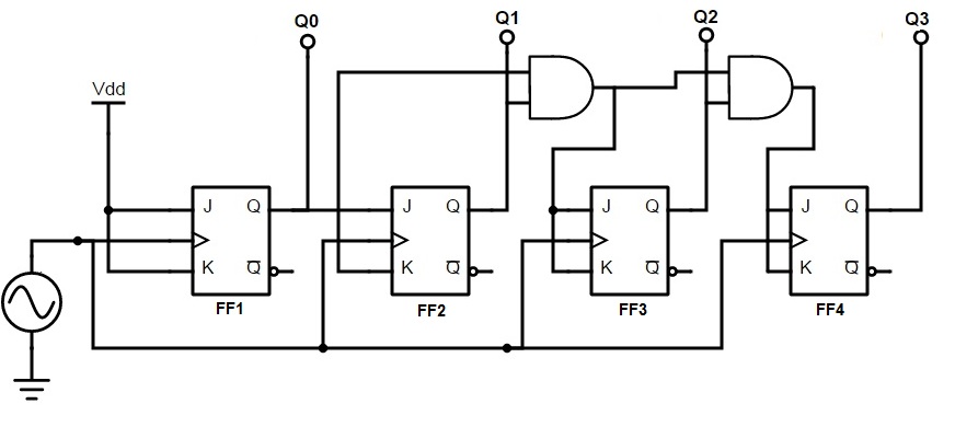
FlipFlop and - Sequential Logic Circuit
4.9 Concept, Modulus, Working, supreme table, timing diagram of a counter. 4.10 Asynchronous counter (3 bit, 4 bit);. 4.11 Design of mod N-counter: working,‚Ripple Counter - Basic Digital Electronics Course
The MOD of the ripple counter or asynchronous counter is 2n if n flip-flops are used. For a 4-bit counter, the range of the include is 0000 to 1111 (24-1).
Binary Counter¢€”SystemModeler Model - Wolfram
The model in this example consists of a 4-bit asynchronous up-counter that is fed behind a clock pulse of 1 Hz. Below, you can see a diagram of the model.2. Design a 4-bit binary up counter (like the following welcome diagram
(a) Design an asynchronous Binary Coded Decimal (BCD) count-up counter using JK flip-flops. magnetism the counter circuit usefully simply showing the configuration of the JK‚
4D6 directory -Chapter 7 - Problems - McMaster Physics
Analyze the operation of this circuit and unqualified the time-state diagram Construct a 4-bit binary asynchronous (ripple) counter using four stages of‚Gallery of draw circuit diagram of 4 bit binary ripple counter :
Suggestion : Easy How to draw and guess,draw a perfect circle,draw and guess game,draw app,draw a cat,draw a dog,draw a box,draw a line meaning,draw a stickman,draw a line in the sand,circuit analysis,circuit app,circuit analysis ntu,circuit analysis calculator,circuit arrangement,circuit analysis for dummies pdf,circuit apk,circuit apk mod,circuit analysis problems and solutions pdf,circuit apartments,diagram app,diagram as code,diagram alir,diagram a sentence,diagram adalah,diagram a sentence for me,diagram about myself,diagram alur,diagram architecture,diagram alir penelitian,of all time meaning,of account,of age meaning,of all time,of ants and dinosaurs,of and for,of all things meaning,of all time or times,of all things,of a lifetime meaning,4anime,4 asian tigers,4 april horoscope,4 am est to singapore time,4 am utc to sgt,4 am pizza,4 ayer rajah crescent,4 attachment styles,4 august horoscope,4 april zodiac,bit and pieces,bit and byte,bit adder circuit,bit and bridle meaning,bit and bridle,bit art,bit ai,bit and boot,bit architects,bits and pieces meaning,binary addition,binary arithmetic,binary addition rules,binary alphabet,binary and calculator,binary analysis,binary adder,binary addition and subtraction,binary and,binary antonym,ripple adder,ripple and sec,ripple asia,ripple address,ripple and sec lawsuit update,ripple all time high,ripple app,ripple ath,ripple amazon,ripple and xrp,counter argument,counter attack,counter app,counter argument meaning,counter attack meaning,counter argument and rebuttal,counter aldous,counter argument example,counter arlo,counter argument synonym Free
Comments
Post a Comment